Assembly
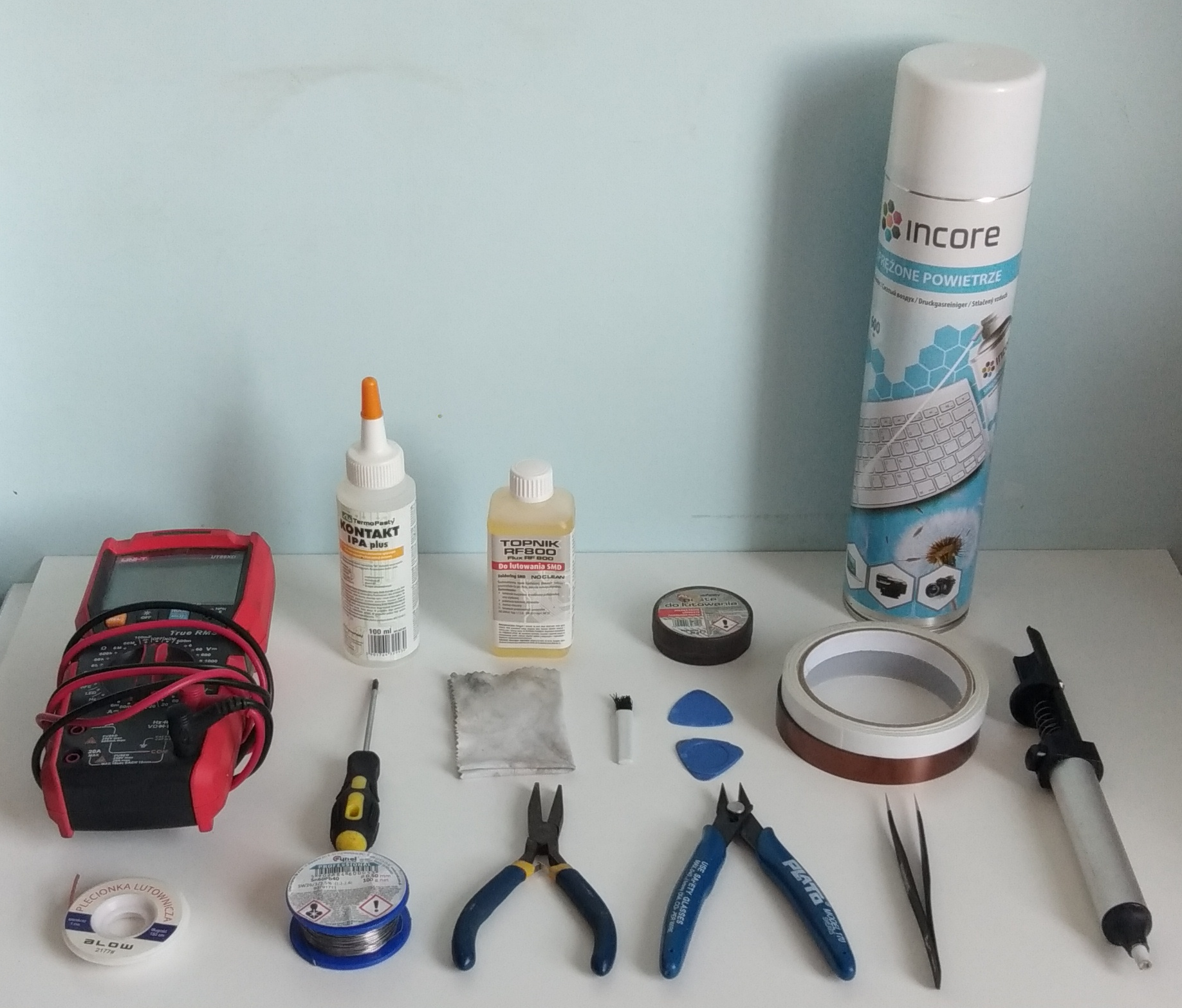
To assemble the handheld, you will need both tools and soldering skills. It would be really cool if you had a hotair station - but in this tutorial I will show you how to assemble the Malinka just with a soldering iron. Tool checklist:
- cutting pliers
- tweezers
- solder (preferably thin and containing lead (Sn60Pb40), I use 0.4mm)
- desoldering wire
- kapton tape
- double sided tape
- flux or soldering paste
- IPA alcohol/isopropanol
- a multimeter (even a cheap one will do)
- a screwdriver
- ESD cloth along with an ESD brush
- third hand and/or PCB holder
- and of course, a soldering iron.
Optional, but really recommended:
- straight pliers
- desoldering pump
- compressed air
- a magnifier
- haribo bears
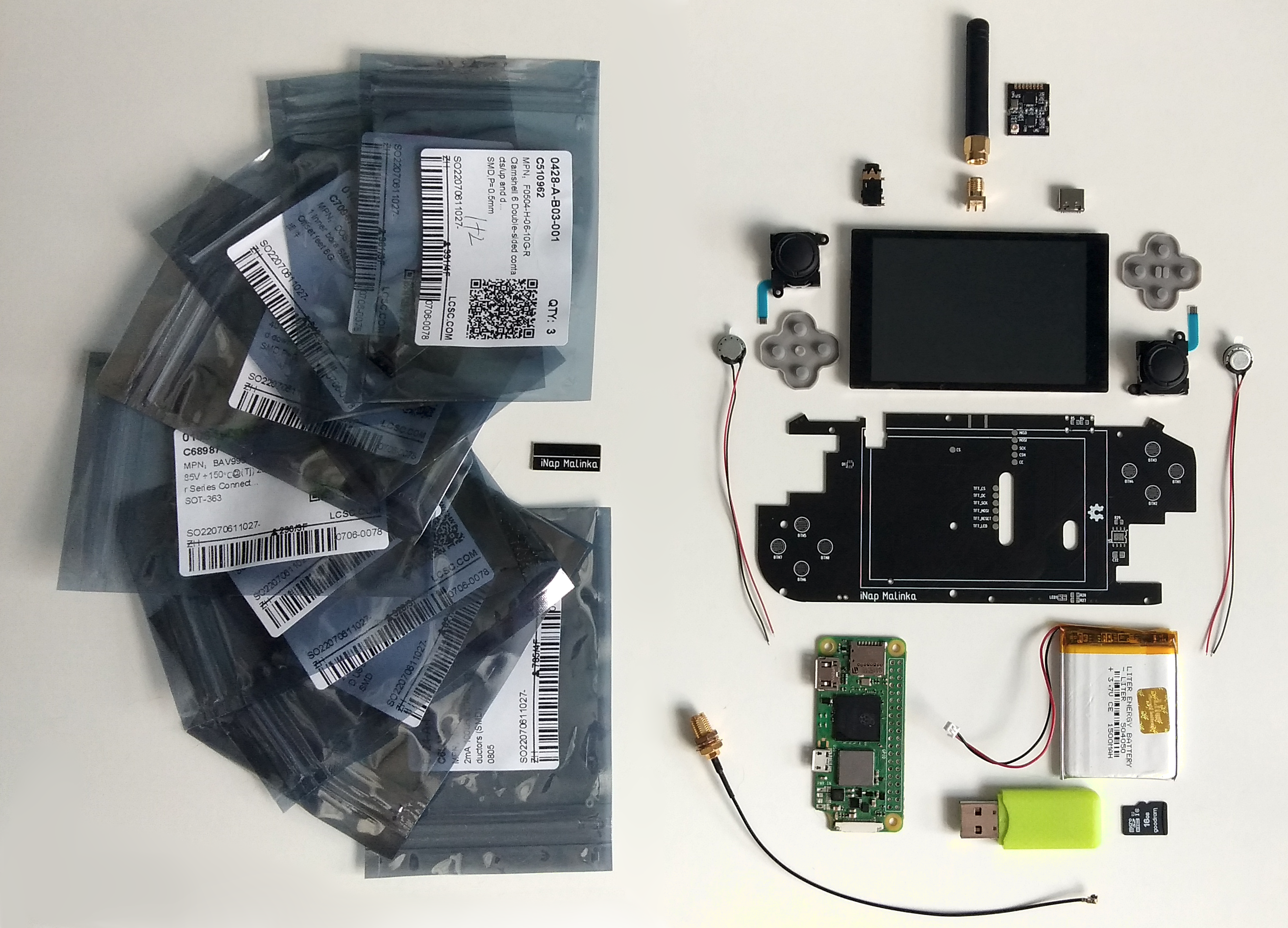
The Bill-Of-Materials is included in the repository. You will also need two M2.5 screws with nuts and washers for the assembly process. Don't forget about the SD card too!
Before starting the assembly process, make sure that you have everything you need - all parts and tools. Remember to print the case, and install system on the Pi before assembling the rest! The assembly process can take up to 6 hours, so prepare a cup of water and haribo bears too, just to keep you motivated during the process. Let's go!
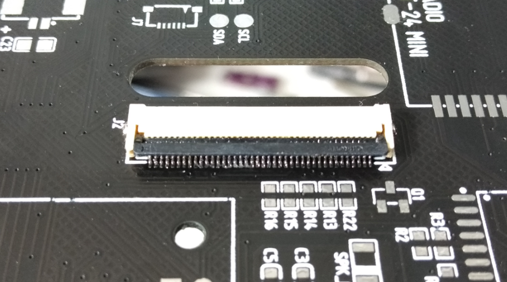
We will begin with the hardest part - just so if you screw up, you won't waste as much time. Preheat your soldering station to your favorite temperature. Mount your PCB so it's rigid and so you can solder it in a comfortable way. Apply a generous amount of solder flux on the pins.
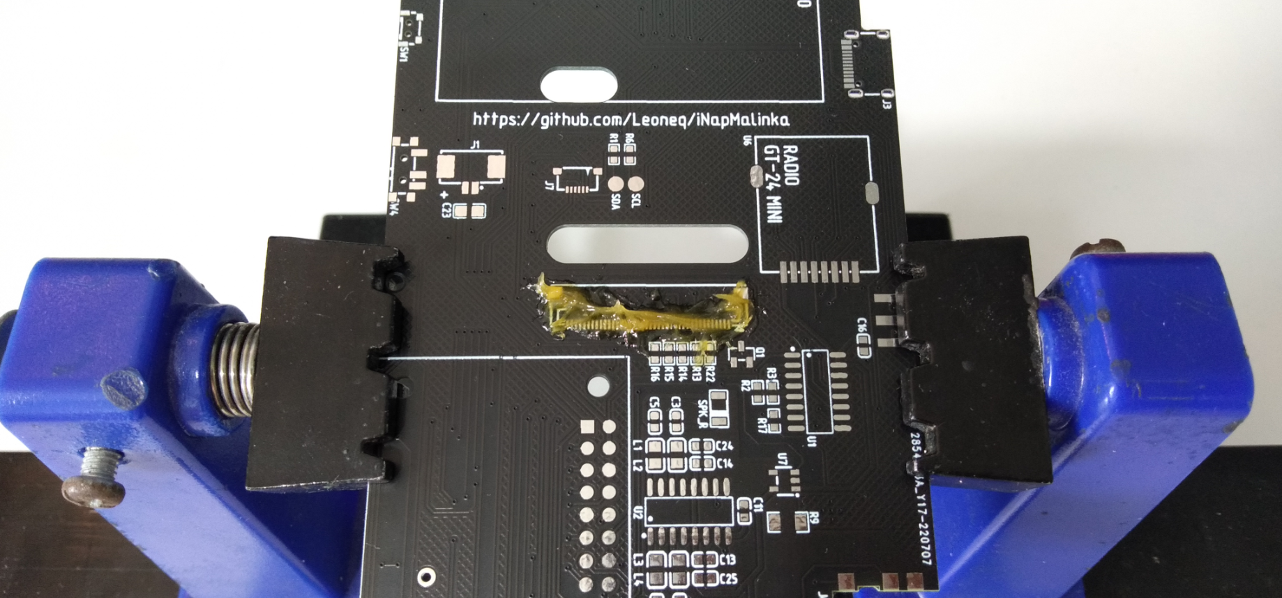
Stick the connector in place, and align it so the pins are meeting the pads almost perfectly. Take your time. If you are sure you did it well, solder one mounting pad on the side of the connector:
Solder the other side too, and check if nothing moved again. If you think everything's fine, then apply solder on all the pins. Basically, you want to make a huge solder bridge like here:
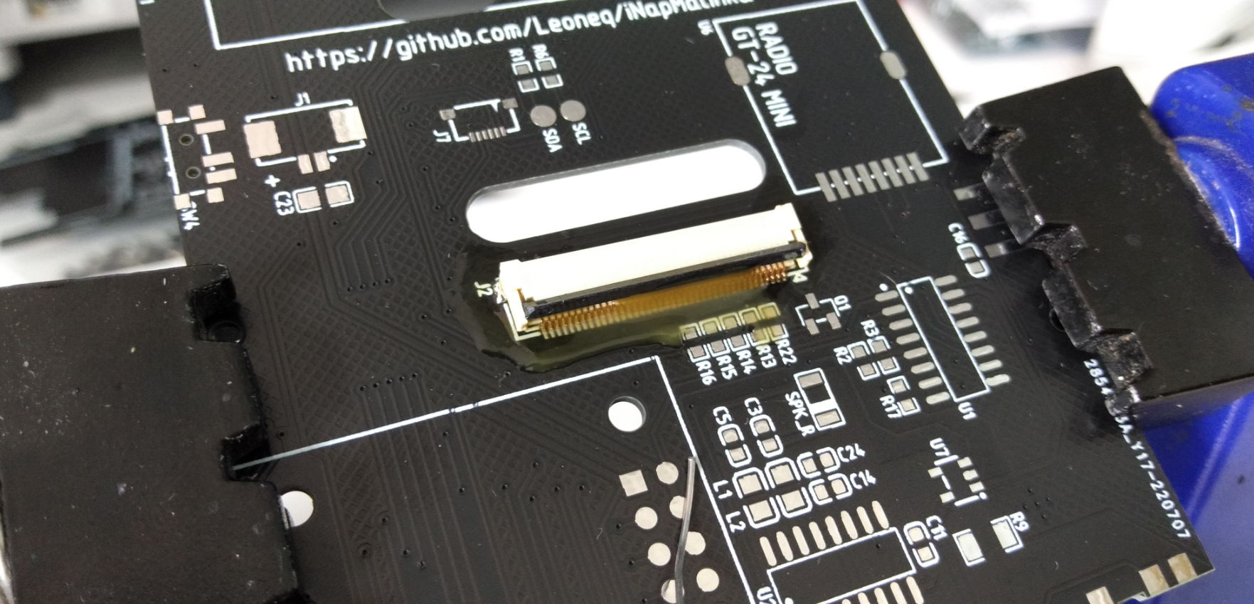
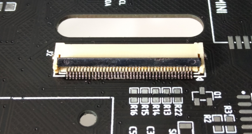
Don't panic if it looks ugly, everything's under control! Take the desoldering wire, and slide it across all the pins. Remember to cut down tinned fragments, and apply more flux if needed.
Once finished, it should look quite neat already. Make sure if there aren't any bridges left, and if so, remove them.
After this step, the connector is basically soldered. Now we need to clean the remaining flux - apply a lot of IPA alcohol, and use a brush and some cloth to remove the remaining flux. It should be removed from the connector and pins, and of course be sure to brush the inside of the connector too. A good approach is to put some alcohol inside, wait a second, and then spray some compressed air inside. No flux can remain inside the connector! Remember to flip the lever during cleaning too.
Once finished, the connector should look pretty good, and no flux should be visible.
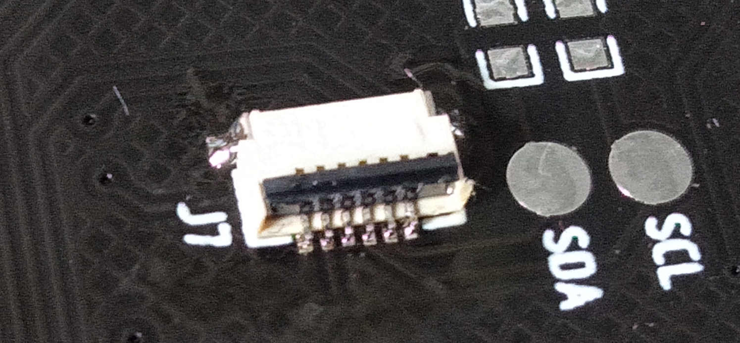
If you made it this far, congratulations! Take a break, and eat a haribo bear. There are only 3 smaller connectors left!! Repeat the process for them too, but if you feel confident, try soldering them just by applying only the necessary amount of solder. Use a magnifier or your phone if you need to see connections more clearly, as I do:
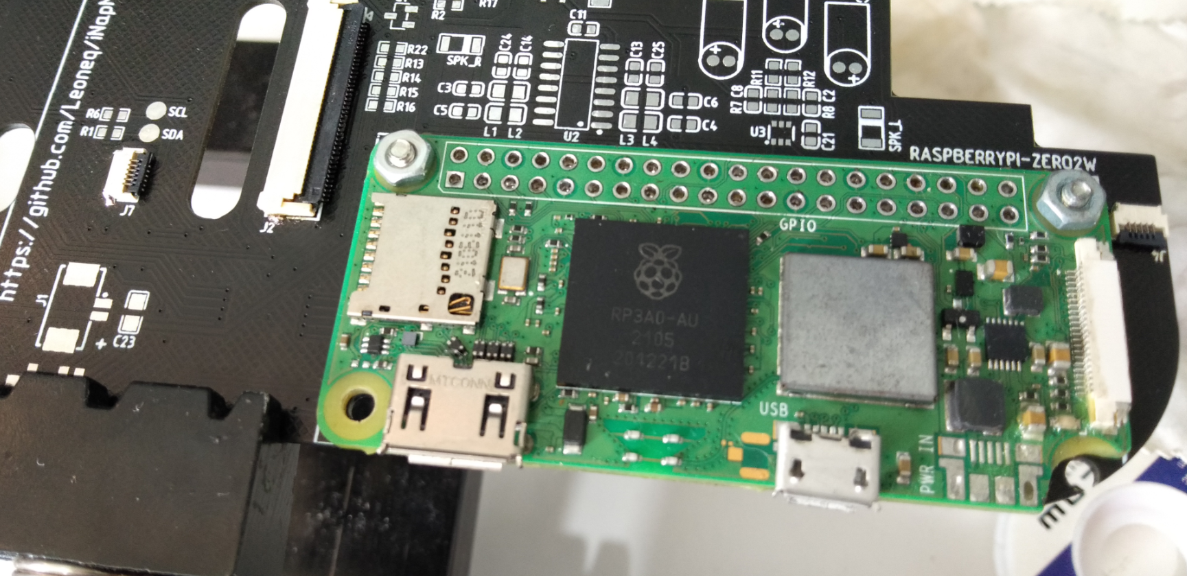
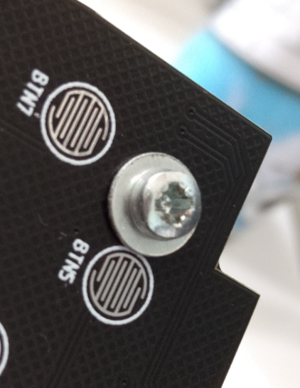
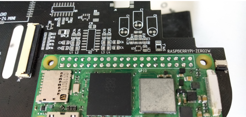
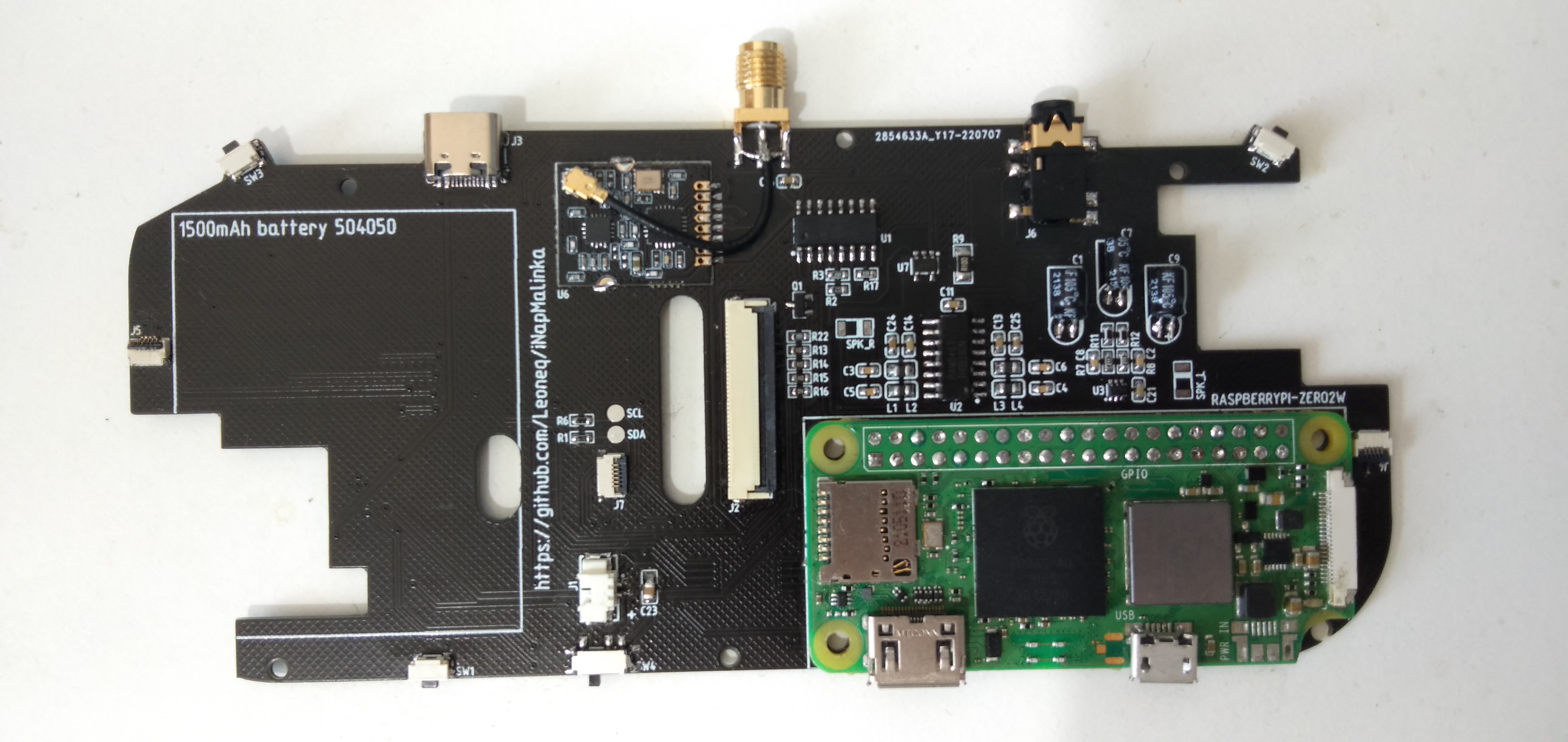
Once we are done with them, the hardest part is over. Time for the semi-hard part - the Raspberry Pi. Don't mind that my Pi is cut in the corner, you don't need to do it. Mount the Pi in it's place using two screws, washers are necessary to not damage the PCB!
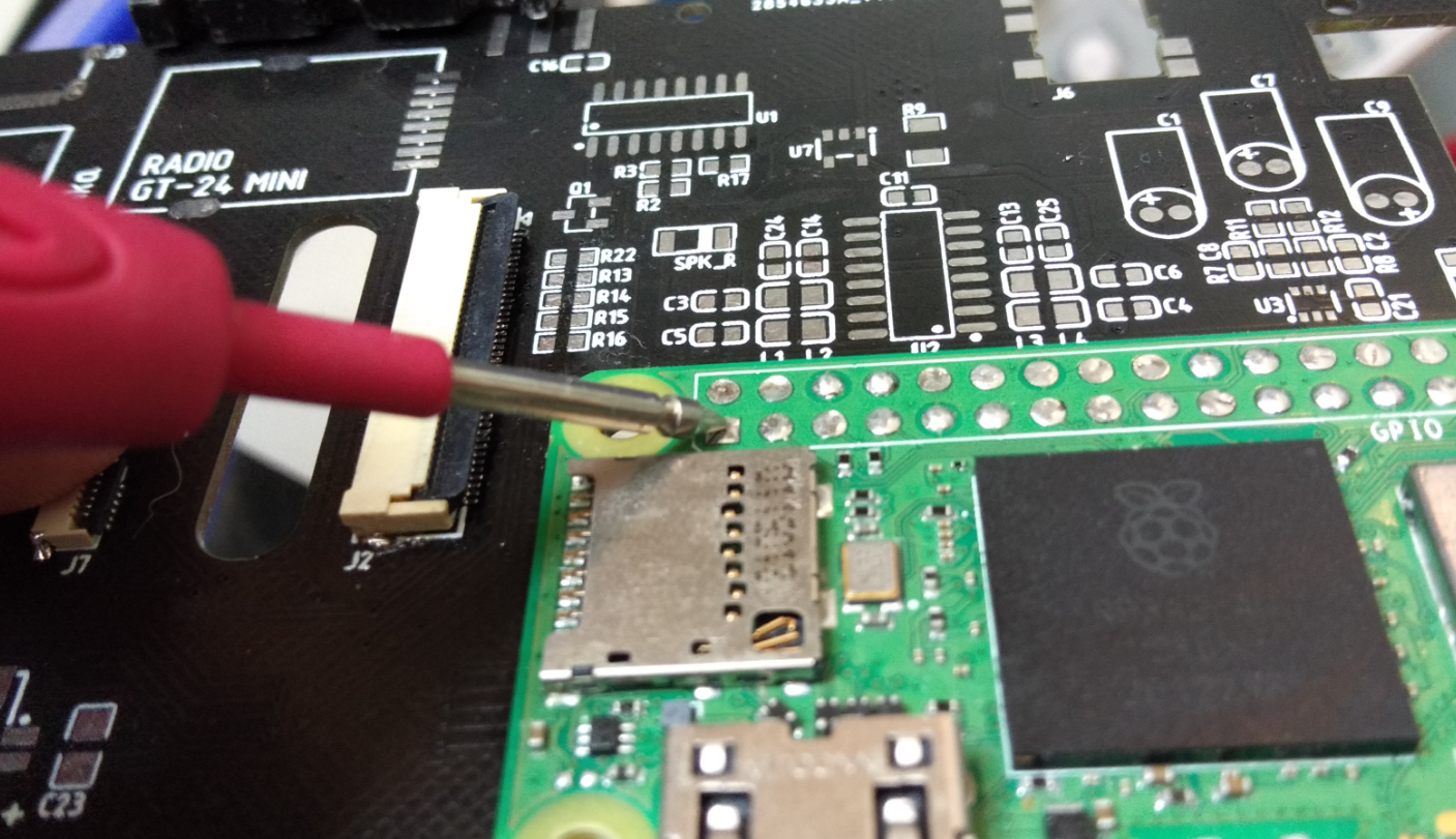
The Pi is surface-mount, which means that soldering it will be quite different. You need to put the tip of soldering iron into the "cup", put some solder on it, and remove the iron. Remember to apply the flux if needed. Repeat the process for the other 39 cups:
Remember to clean it of remaining flux using IPA, cloth, and brush. This is also a good moment to desolder the power USB, as we don't need it. Do it very carefully. Once you think you're done, you must check if you have soldered all the pads correctly. Use some common pins and exposed pads for that, and check along with this list (first 3.3v pin is the square one):
3.3v,       VBAT
I2C_SDA,    VBAT
I2C_SCL,    GND
RADIO_CE,   BTN_SELECT
GND,        BTN_UP
MCP_CS,     RADIO_CSN
BTN_LT,     GND
BTN_LEFT,   BTN_RIGHT
3.3v,       TFT_DC
TFT_MOSI,   GND
BTN_Y,      TFT_RESET
TFT_SCK,    TFT_CS
GND,        BTN_DOWN
BTN_RT,     BTN_A
BTN_B,      GND
BTN_X,      SOUND_L
SOUND_R,    GND
RADIO_MISO, BTN_START
TFT_LED,    RADIO_MOSI
GND,        RADIO_SCK
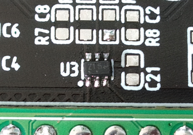
Once you're done with the Pi, and all connections are checked and fixed, it's time for another haribo bear(s). Now only small SMD components are left - let's begin with smallest U3 - tin one corner pad:
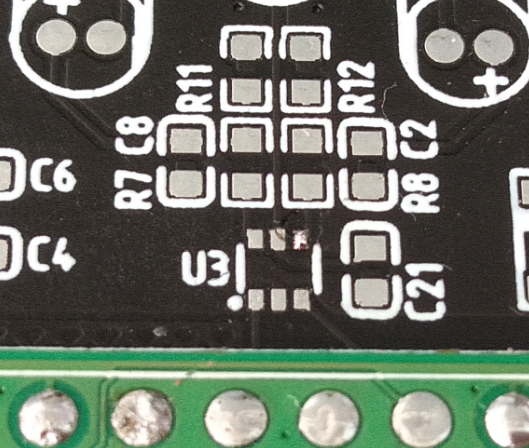
Mount and align the IC properly. Spot that the dots are indicating the first pin - the dot on the IC must match the dot on the PCB!
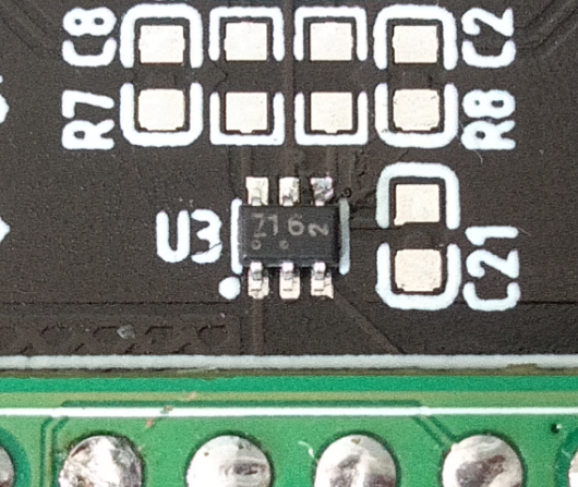
Solder the other corner, and all the remaining pins. As you can see, my IC twisted a little but it's fine as long as connections are correct:
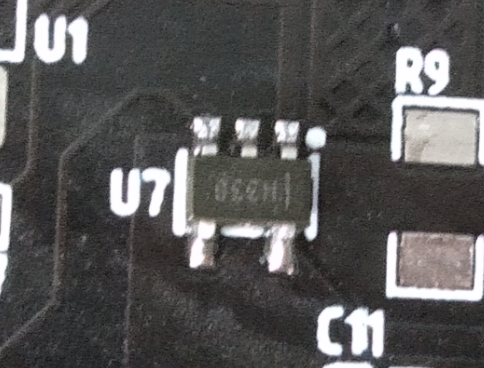
Remember to take your time, and apply a lot of flux. Repeat the process for the U7, Q1, U1 and U2:
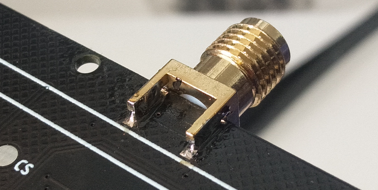
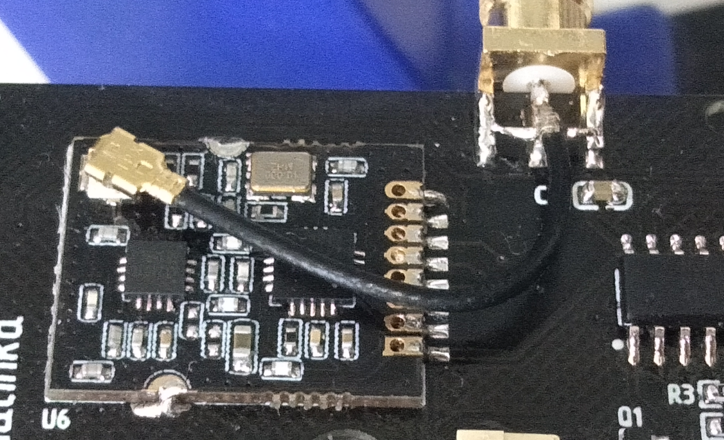
Now we will attach the radio module. If you don't want to use radio at all, you can omit soldering it, as well as the SMA connector. Once again, tin and align using one pad:
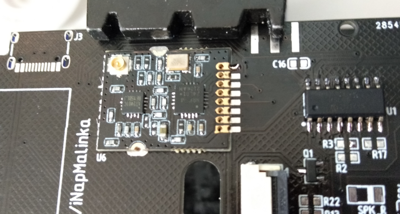
Apply even more flux, and when pressing the module into the main board, solder the mounting pad. It will keep the module flat and attached well.
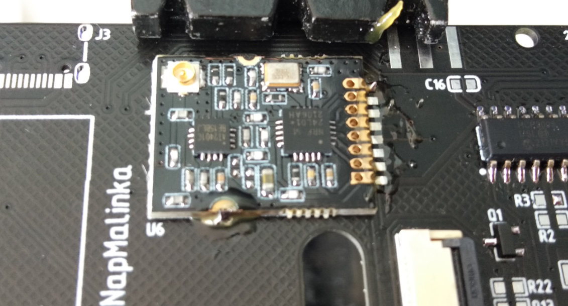
Solder the rest of the pins, and voila! This is the result you should have so far: (note: this is a picture of an older version, you need to solder R10, C12, C10 and R18 near the U2 too!)
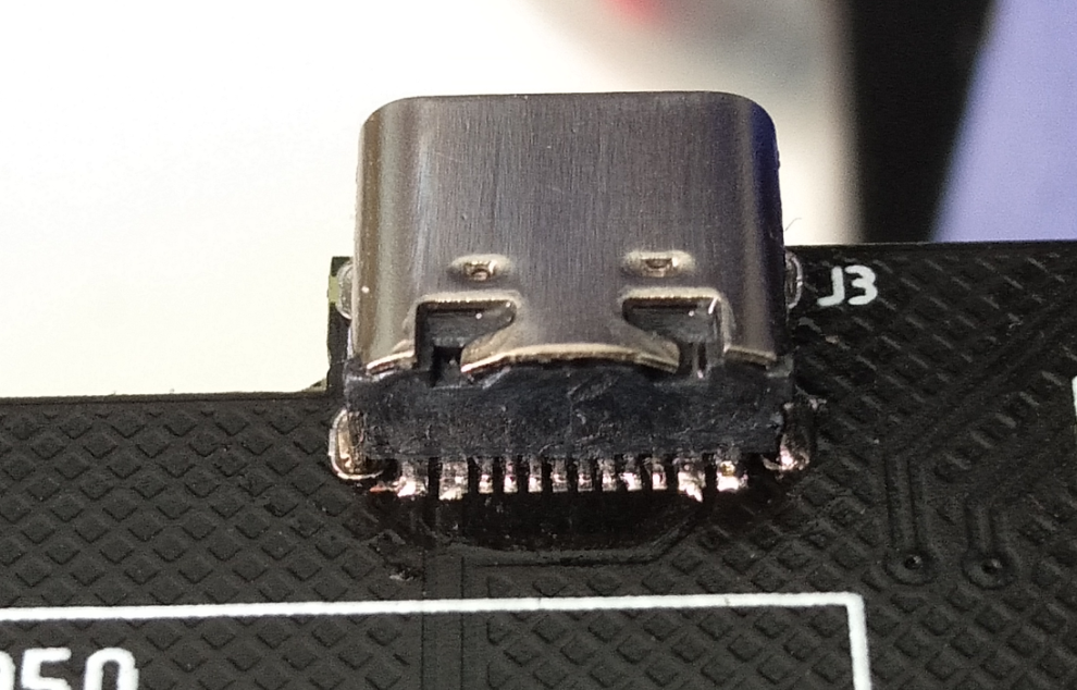
It's time to solder the connectors. The process is quite repetitive, as again, we need to attach the connector using one pad.
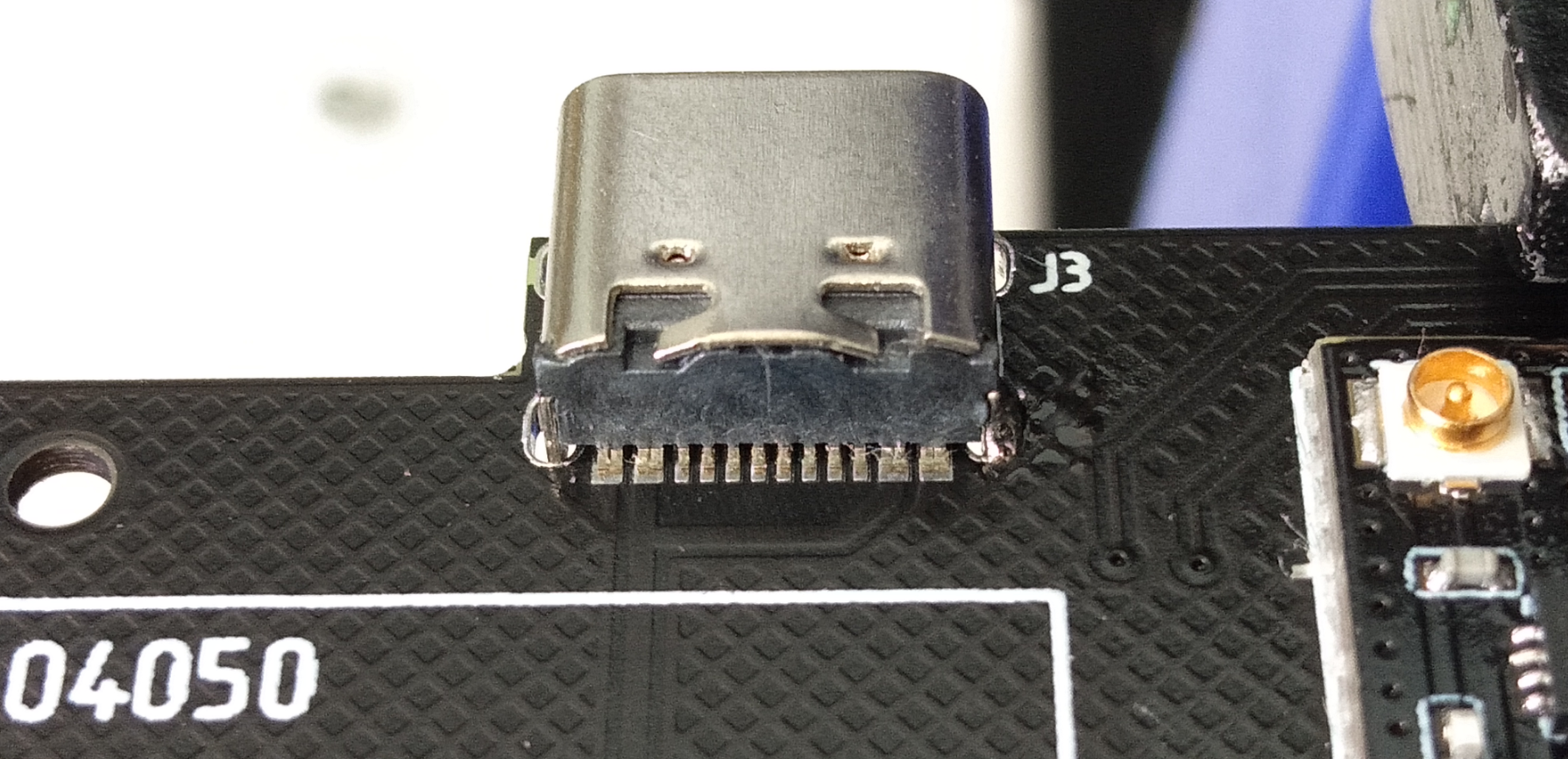
Solder other pads (but for this USB-C connector, they must remain flat as LCD goes in top of them!
And all you need to do is tin other pins as well.
Make a similar thing with the SMA connector. It's meant to be mounted on the edge of thicker boards, so make sure it's flat on the radio side, and "floating" on the screen side:
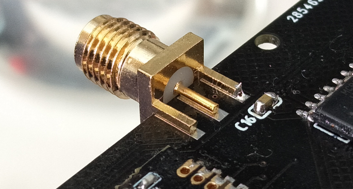
You will need to apply a little bit more solder to connect it on the other side as well.
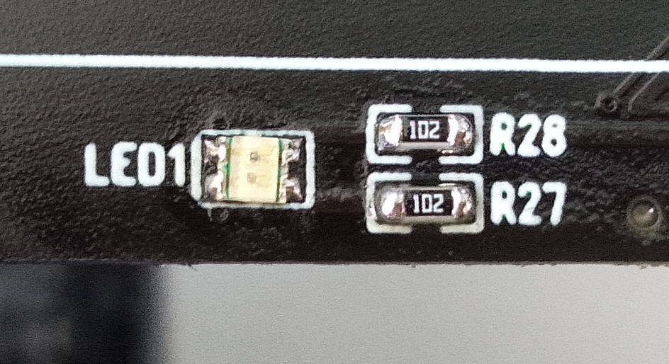
We will move our focus to an LED now. On it's underside, there's a green line indicating the cathode. That line must be facing the "LED1" label:
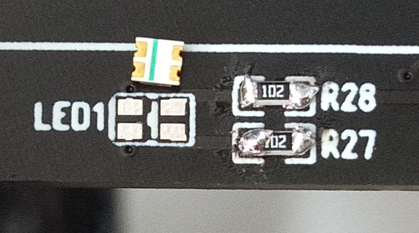
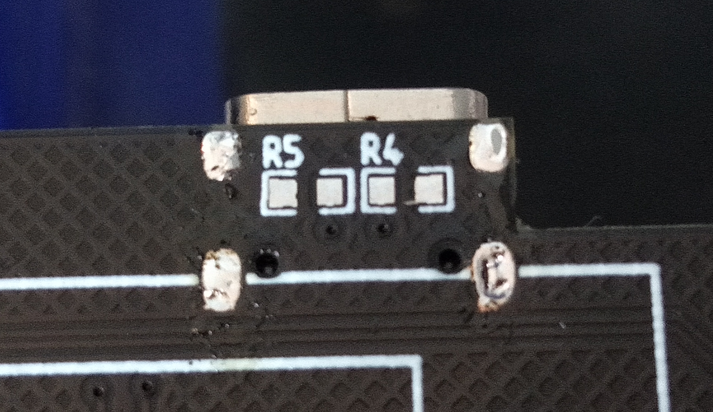
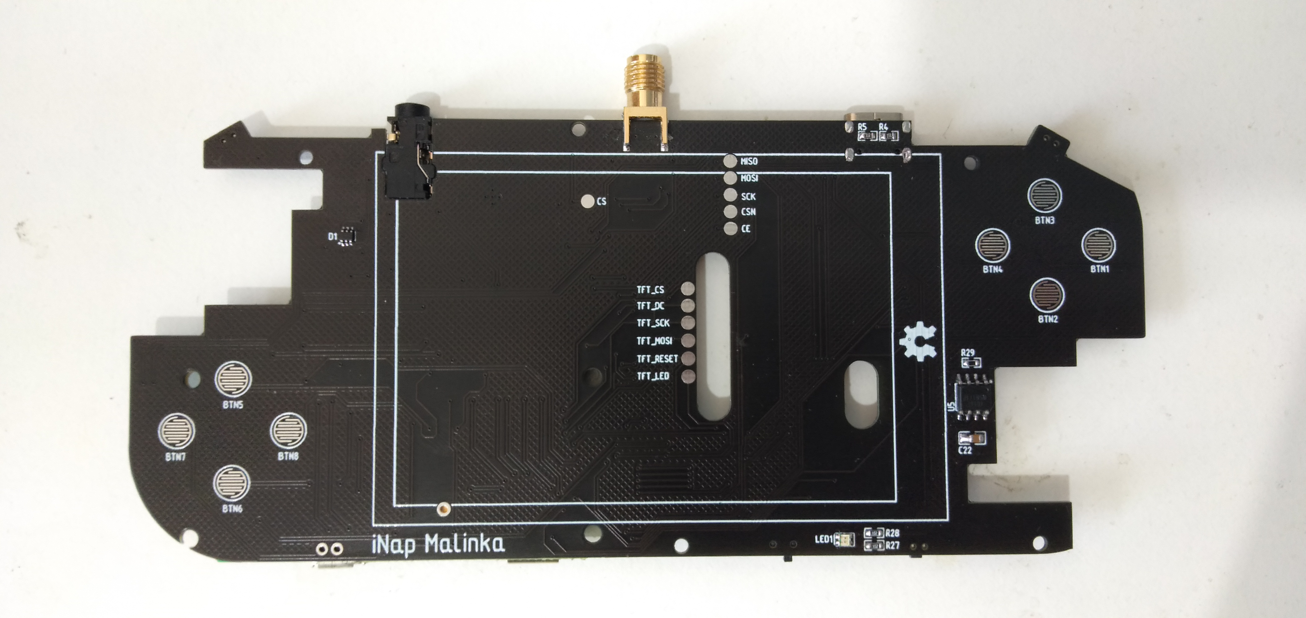
Solder the resistors too. Follow the schematic to check all components' places!
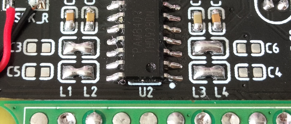
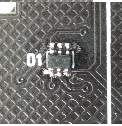
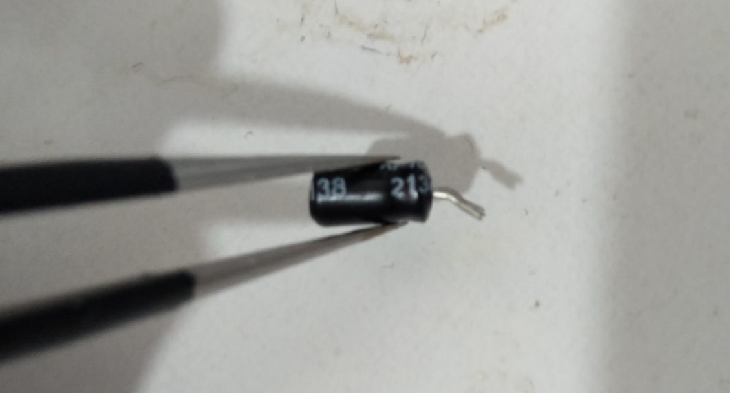
Continue soldering the passive components, and don't forget about the D1 in the top left corner. A note here though, DO NOT solder L1-L4, or C3-C6 yet. Leave C3-C6 free and short L1-L4 as pictured. You can add them once your sound turns out to be of poor quality.
Keep those elements in case your audio ends up being poor quality.
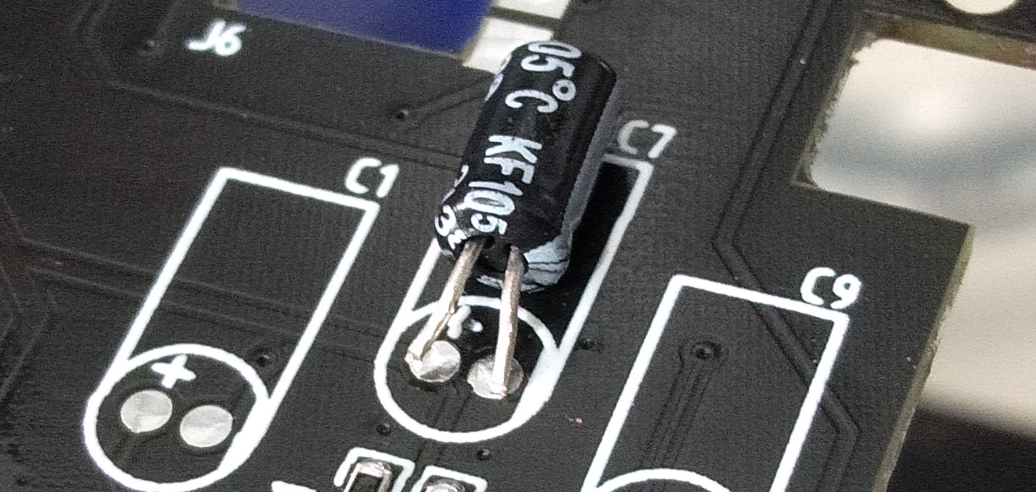
The audio capacitors are surface-mount too, despite being THT. Just cut their leads as shown:
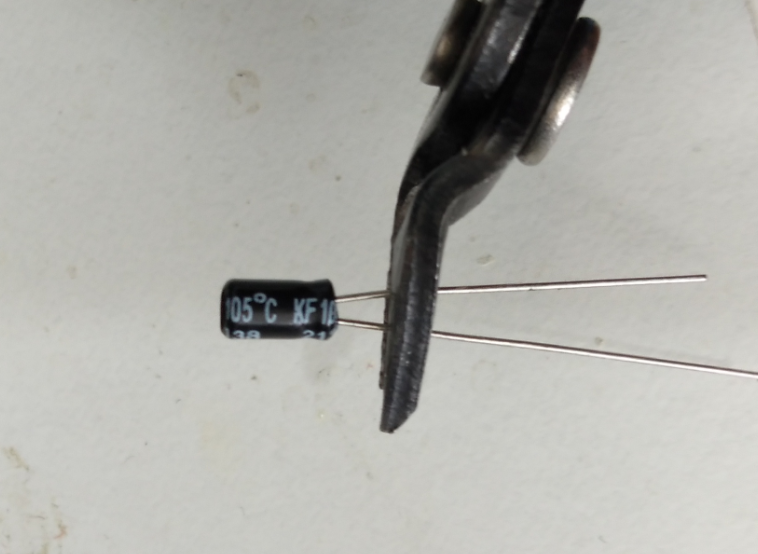
Bend them down:
And attach in place. The blue/gray strip on them indicates the cathode (minus side). The other one goes on the plus! Make EXTRA sure that you haven't swapped their leads, or else they won't work properly.
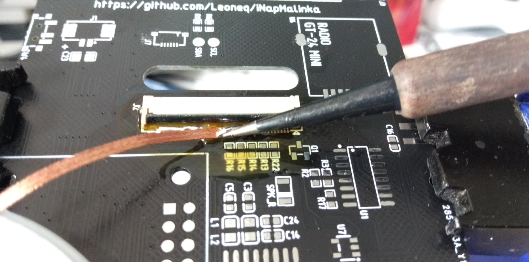
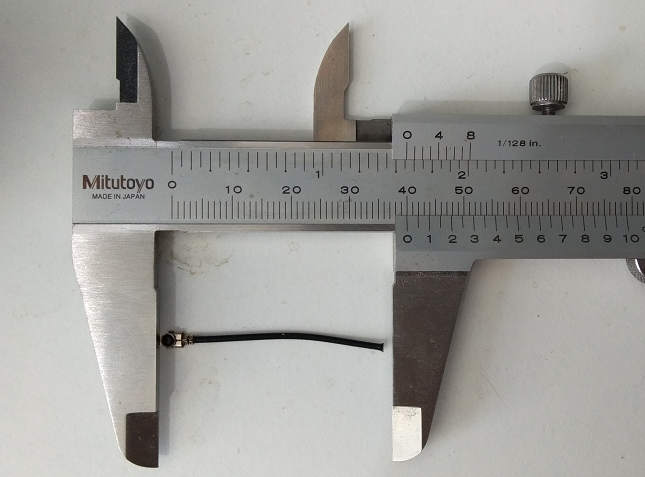
One of the last things to do is to connect the radio module with the SMA connector. There's a small IPX connector on it, so I grabbed myself a small kit with a coaxial wire and an SMA antenna. NOTE: That antenna is meant for GSM, not 2.4GHZ! It needs to be tested, so be careful. Cut it down to about 40mm in length, or whatever is suitable for your setup:
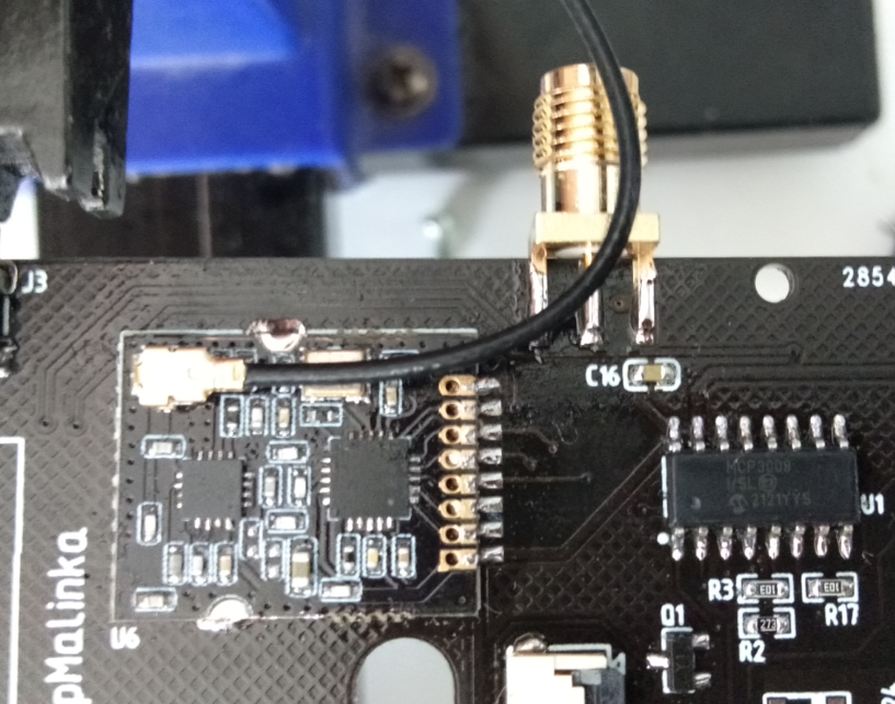
Very carefully strip the coaxial wire so the core and shield are exposed well. Make some kind of a "cross" shape as shown:
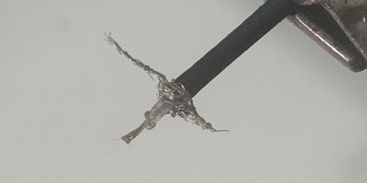
Tin it (and make sure to not make bridges!)
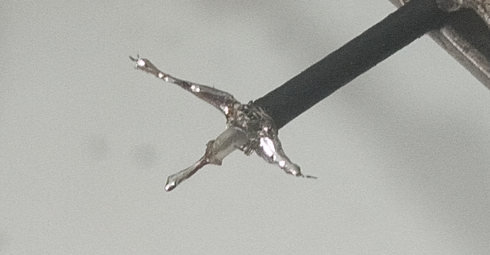
Solder it symmetrically, and once again make extra sure that the core isn't shorted to the shield. Use a multimeter to check it!
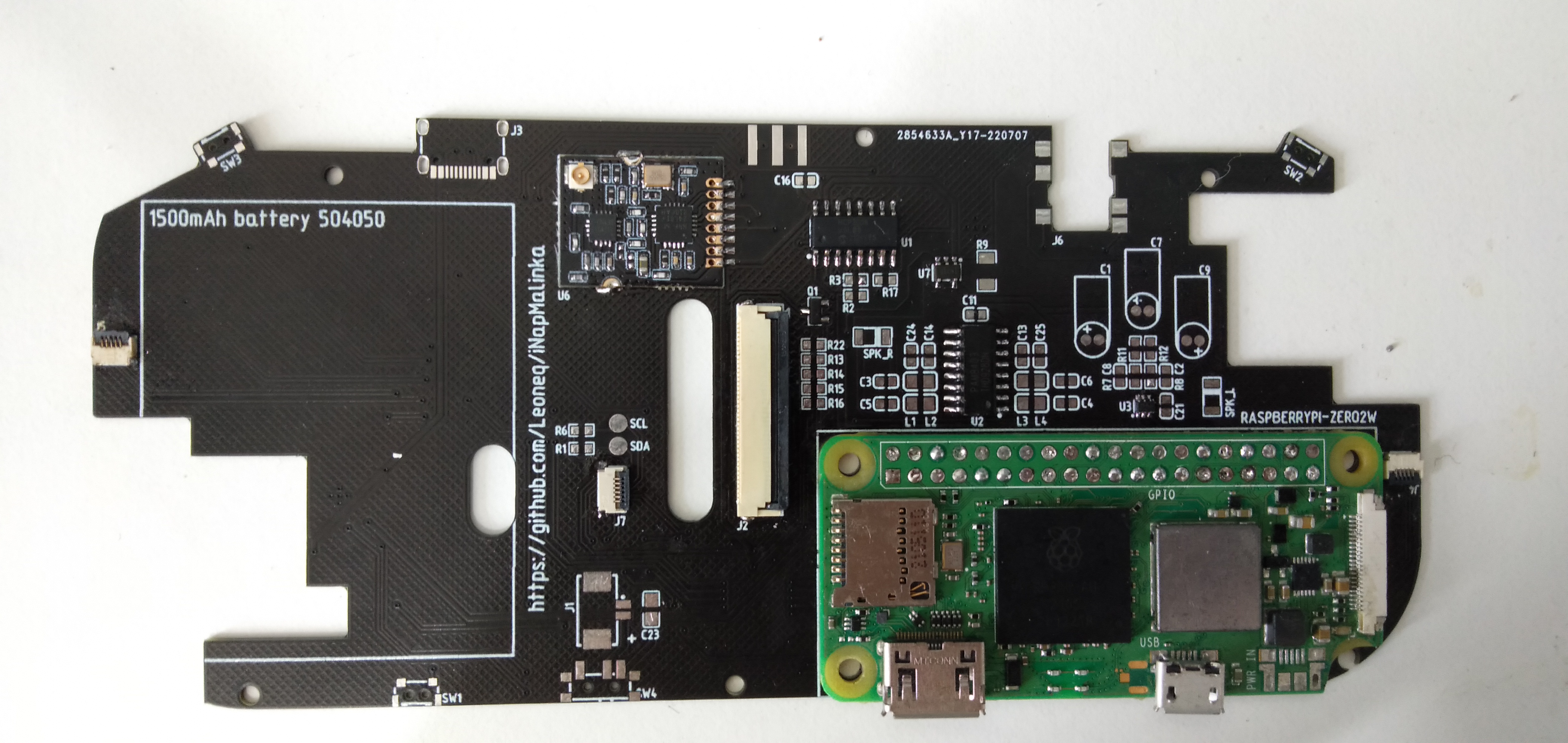
This is another checkpoint. Eat some more haribos. We can boot up the Pi already! Make sure that your board looks just like this one:
If you feel confident about your beautiful work, insert the SD card you prepared earlier. If everything goes fine, the green LED should start blinking. If not, well... welcome to the club of having a fried pi.
Just kidding, check if you connected the battery properly, if your SD card is all good, and try to maybe flip the switch. Once you finally got your Pi working, log in via the SSH and type in sudo shutdown now. After a minute or two, flip the switch off and remove the battery.
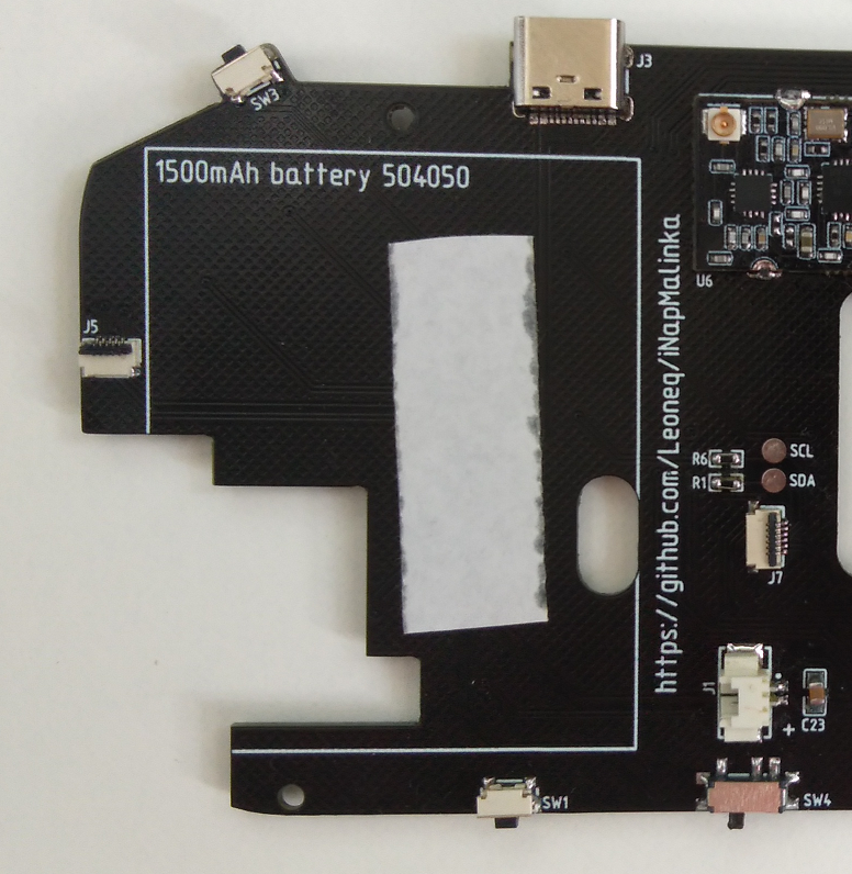
Everything you see is exposed and goes under the screen, you must hide with a piece of kapton tape : audio jack, all test pads, as well as part of the USB C connector. Stick some double-sided tape too:

Do a similar thing for the battery.
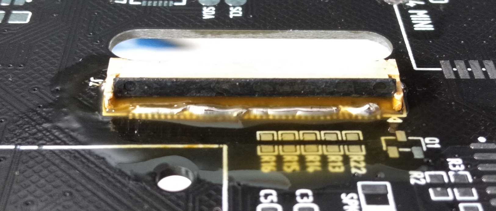
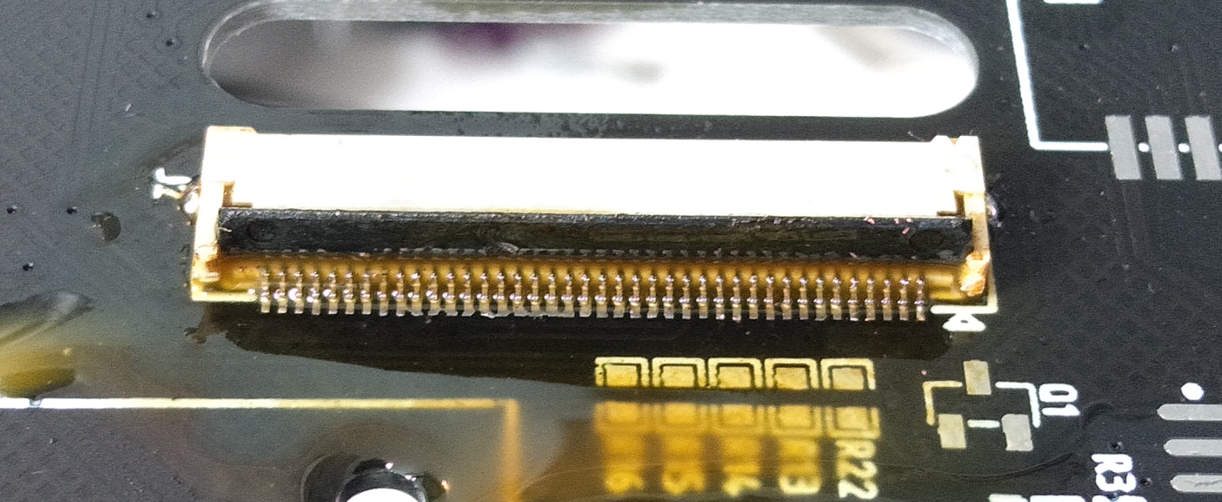
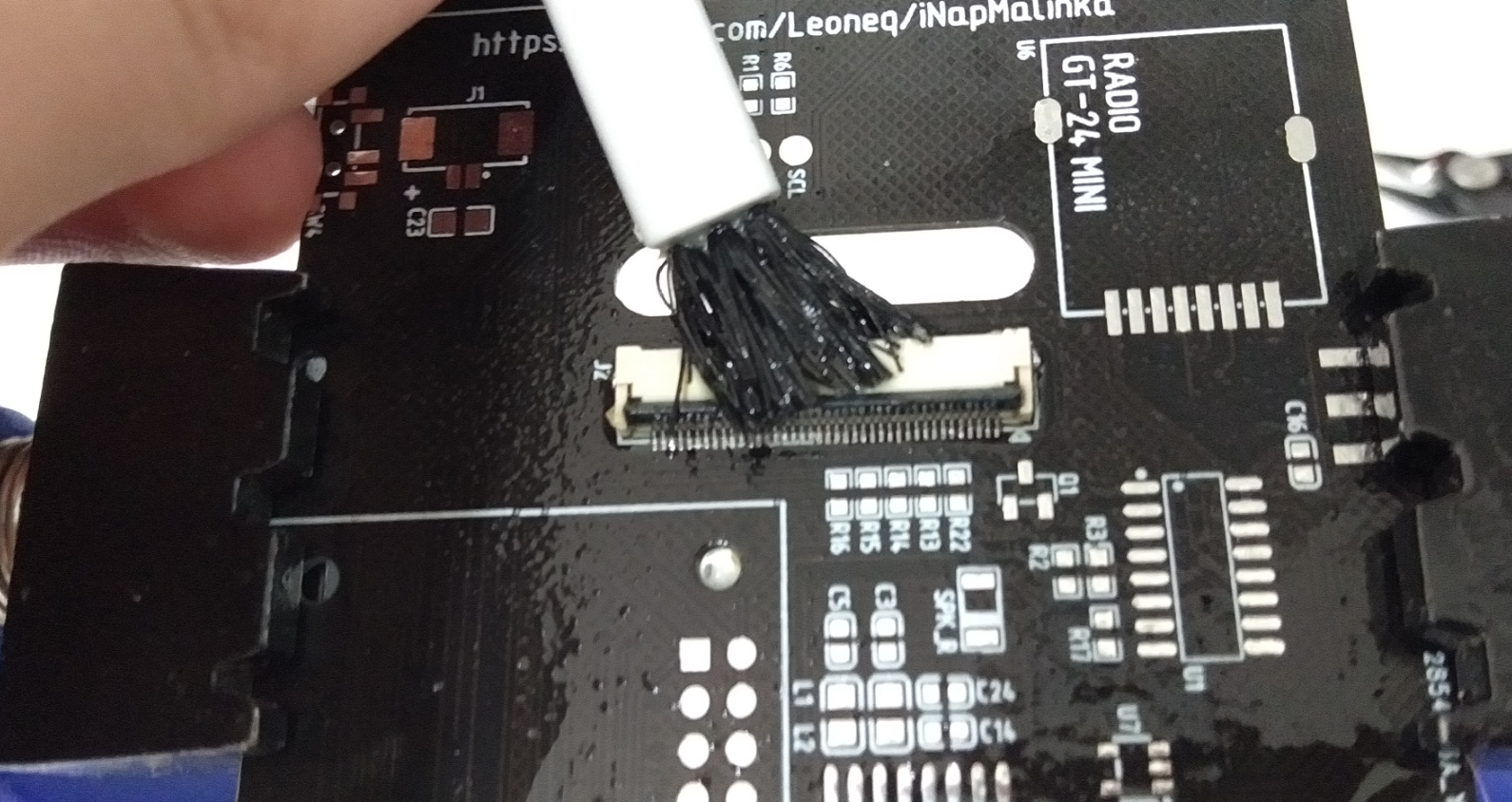
Now, open the connector levers and very carefully slide the large ribbon through the hole. Use tweezers to push it inside the connector, and once it's properly aligned, close the lever. Do a similar thing with the smaller ribbon too. The backside of the PCB should look like this:

But don't stick the screen yet, we will do that soon! One of the last things to do is to prepare the speakers. Cut the wire on one speaker so it matches the shorter one in the picture below, and use those wires to expand the second speaker. Once you're done, twist the wires so they look just like they do in the reference below. The shorter speaker goes to SPK_L and longer one to SPK_R.

Aaaaaaand we're done! Insert the battery and turn the Malinka on. If you can see that the screen shows EmulationStation after few seconds, there's nothing left but to attach it with the double-sided tape. If you don't see any picture, head to the troubleshooting page.


Shutdown the Pi again, and detach the battery. Push the controller buttons and check if they're sliding smoothly - they must slide smoothly.

Put the rubber pads on them. You can see that they're not symmetrical, one side is 1mm longer - make it parallel to the longer edge of the PCB (horizontal).

Don't forget about side buttons too! Make sure to slide the switch to the left.

Now, very carefully, push the PCB inside. The SMA connector should go all the way through the hole. The rubber pads must remain in place!

Press the PCB down. The USB connector on the Pi should 'jump' into the place, and power switch should be matched too.


Inspect the alignment of the rubber pads. Fix them if they're not in place - you can easily detect that by pressing button and "feeling something wrong"

Put the joysticks on place, and screw them but don't use too much force!!! The plastic mounts on them are really thin and too much torque can break them. Stop once you feel more resistance.


Pull up the lever, and even more carefully slide the ribbon inside using tweezers. The joysticks have carbon paths so they will wear out after 3 or 4 insertions. Once in place, you probably don't want to disconnect them.

Time for the triggers. A trigger in place should look like this:

The backside should look as shown. If the cables are getting over mounting holes, secure them using kapton tape.

Finally, gently push in the cover, making sure that triggers are still in place. The 6 screws shouldn't stick out at all.

This is how the finished product should look like!!

Head to the user guide to learn how to use Malinka!